$1.5 Billion Worldwide E-Beam Wafer Inspection System Industry to 2027 - Players Include Aerotech, Applied Materials, ASML Holding and Hitachi

Global E-Beam Wafer Inspection System Market
Dublin, Jan. 24, 2023 (GLOBE NEWSWIRE) -- The "E-Beam Wafer Inspection System Market: Global Industry Trends, Share, Size, Growth, Opportunity and Forecast 2022-2027" report has been added to ResearchAndMarkets.com's offering.
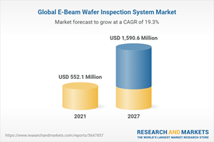
The global e-beam wafer inspection system market size reached US$ 552.1 Million in 2021. Looking forward, the publisher expects the market to reach US$ 1,590.6 Million by 2027, exhibiting a CAGR of 19.29% during 2021-2027.
Keeping in mind the uncertainties of COVID-19, we are continuously tracking and evaluating the direct as well as the indirect influence of the pandemic on different end use industries. These insights are included in the report as a major market contributor.
E-beam wafer inspection system refers to a semiconductor fabrication tool based on electron beam scanning of integrated circuit (IC) components or wafers. It is used for detecting any defects in the wafers before final packaging and is ideal for scanning small sections of a die to identify specific hard-to-detect systematic and random defects.
The inspection system scans the wafer and determines coordinates of the defects by comparing it to the image of the adjacent dies. This technique is commonly used while manufacturing compact gadgets, smartphones, laptops and tablets. It is also used for lithographic qualification, wafer dispositioning and reticle quality optimization.
Significant growth in the electronics industry, along with rapid industrialization, is one of the key factors creating a positive outlook for the market. Semiconductor wafers are widely used for manufacturing specialized devices and consumer electronics, thereby increasing the demand for efficient inspection systems.
Furthermore, the electrification and automation in automobiles is also driving the market growth. Numerous kinds of wafers are used in automobile components, such as airbag controls, global positioning systems (GPS), anti-lock braking systems (ABS), navigation and display systems and power down and window controls.
They are also used for improving automated driving and collision detection technologies, which, in turn, have increased the demand for wafer inspection systems. Moreover, various technological advancements, such as the development of multi-beam e-beam inspection systems that are more efficient and minimize the overall time required for mass production, are projected to drive the market further.
Competitive Landscape:
The report has also analysed the competitive landscape of the market with some of the key players being Aerotech Inc., Applied Materials Inc., ASML Holding N.V., Hitachi Ltd., KLA-Tener Corporation, Lam Research Corporation, Nanotronics Imaging Inc., NXP Semiconductors N.V. (Qualcomm Incorporated), Renesas Electronics Corporation, Synopsys Inc., Taiwan Semiconductor and Teledyne Technologies.
Key Questions Answered in This Report:
How has the global e-beam wafer inspection system market performed so far and how will it perform in the coming years?
What has been the impact of COVID-19 on the global e-beam wafer inspection system market?
What are the key regional markets?
What is the breakup of the market based on the resolution?
What is the breakup of the market based on the application?
What is the breakup of the market based on the end use?
What are the various stages in the value chain of the industry?
What are the key driving factors and challenges in the industry?
What is the structure of the global e-beam wafer inspection system market and who are the key players?
What is the degree of competition in the industry?
Report Attribute | Details |
No. of Pages | 142 |
Forecast Period | 2021 - 2027 |
Estimated Market Value (USD) in 2021 | $552.1 Million |
Forecasted Market Value (USD) by 2027 | $1590.6 Million |
Compound Annual Growth Rate | 19.2% |
Regions Covered | Global |
Key Topics Covered:
1 Preface
2 Scope and Methodology
3 Executive Summary
4 Introduction
4.1 Overview
4.2 Key Industry Trends
5 Global E-Beam Wafer Inspection System Market
5.1 Market Overview
5.2 Market Performance
5.3 Impact of COVID-19
5.4 Market Forecast
6 Market Breakup by Resolution
6.1 Less than 1 nm
6.1.1 Market Trends
6.1.2 Market Forecast
6.2 1 nm to 10 nm
6.2.1 Market Trends
6.2.2 Market Forecast
6.3 More than 10 nm
6.3.1 Market Trends
6.3.2 Market Forecast
7 Market Breakup by Application
7.1 Defect Imaging
7.1.1 Market Trends
7.1.2 Market Forecast
7.2 Lithographic Qualification
7.2.1 Market Trends
7.2.2 Market Forecast
7.3 Bare Wafer OQC/IQC
7.3.1 Market Trends
7.3.2 Market Forecast
7.4 Wafer Dispositioning
7.4.1 Market Trends
7.4.2 Market Forecast
7.5 Reticle Quality Inspection
7.5.1 Market Trends
7.5.2 Market Forecast
7.6 Inspector Recipe Optimization
7.6.1 Market Trends
7.6.2 Market Forecast
8 Market Breakup by End Use
8.1 Communication Devices
8.1.1 Market Trends
8.1.2 Market Forecast
8.2 Consumer Electronic Equipment
8.2.1 Market Trends
8.2.2 Market Forecast
8.3 Automotive Parts
8.3.1 Market Trends
8.3.2 Market Forecast
8.4 Others
8.4.1 Market Trends
8.4.2 Market Forecast
9 Market Breakup by Region
10 SWOT Analysis
11 Value Chain Analysis
12 Porters Five Forces Analysis
13 Price Analysis
14 Competitive Landscape
14.1 Market Structure
14.2 Key Players
14.3 Profiles of Key Players
14.3.1 Aerotech Inc.
14.3.1.1 Company Overview
14.3.1.2 Product Portfolio
14.3.2 Applied Materials Inc.
14.3.2.1 Company Overview
14.3.2.2 Product Portfolio
14.3.2.3 Financials
14.3.2.4 SWOT Analysis
14.3.3 ASML Holding N.V.
14.3.3.1 Company Overview
14.3.3.2 Product Portfolio
14.3.3.3 Financials
14.3.3.4 SWOT Analysis
14.3.4 Hitachi Ltd.
14.3.4.1 Company Overview
14.3.4.2 Product Portfolio
14.3.4.3 Financials
14.3.4.4 SWOT Analysis
14.3.5 KLA-Tener Corporation
14.3.5.1 Company Overview
14.3.5.2 Product Portfolio
14.3.5.3 Financials
14.3.5.4 SWOT Analysis
14.3.6 Lam Research Corporation
14.3.6.1 Company Overview
14.3.6.2 Product Portfolio
14.3.6.3 Financials
14.3.6.4 SWOT Analysis
14.3.7 Nanotronics Imaging Inc.
14.3.7.1 Company Overview
14.3.7.2 Product Portfolio
14.3.8 NXP Semiconductors N.V. (Qualcomm Incorporated)
14.3.8.1 Company Overview
14.3.8.2 Product Portfolio
14.3.8.3 Financials
14.3.8.4 SWOT Analysis
14.3.9 Renesas Electronics Corporation
14.3.9.1 Company Overview
14.3.9.2 Product Portfolio
14.3.9.3 Financials
14.3.9.4 SWOT Analysis
14.3.10 Synopsys Inc.
14.3.10.1 Company Overview
14.3.10.2 Product Portfolio
14.3.10.3 Financials
14.3.10.4 SWOT Analysis
14.3.11 Taiwan Semiconductor
14.3.11.1 Company Overview
14.3.11.2 Product Portfolio
14.3.11.3 Financials
14.3.11.4 SWOT Analysis
14.3.12 Teledyne Technologies
14.3.12.1 Company Overview
14.3.12.2 Product Portfolio
14.3.12.3 Financials
14.3.12.4 SWOT Analysis
For more information about this report visit https://www.researchandmarkets.com/r/j470zz
Attachment
CONTACT: CONTACT: ResearchAndMarkets.com Laura Wood,Senior Press Manager press@researchandmarkets.com For E.S.T Office Hours Call 1-917-300-0470 For U.S./ CAN Toll Free Call 1-800-526-8630 For GMT Office Hours Call +353-1-416-8900

